
Prize: $10 PCB production grant + 1 snowflake
- Setup EasyEDA
- Creating a Project in EasyEDA
- Schematic Editor
- PCB Editor (Setting Up Multicolor Silkscreen)
- Design Your Ornament
- Ordering the Board
Head over to EasyEDA and create an account if you haven’t already. EasyEDA is a web-based PCB design tool that supports multicolor silkscreen printing through JLCPCB and this is why we’ll be using it for our project.
You’re free to use your preferred EDA software, though keep in mind that multicolor silkscreen may not be supported in all platforms. (There are some plugins for kicad but I have not tested them myself)
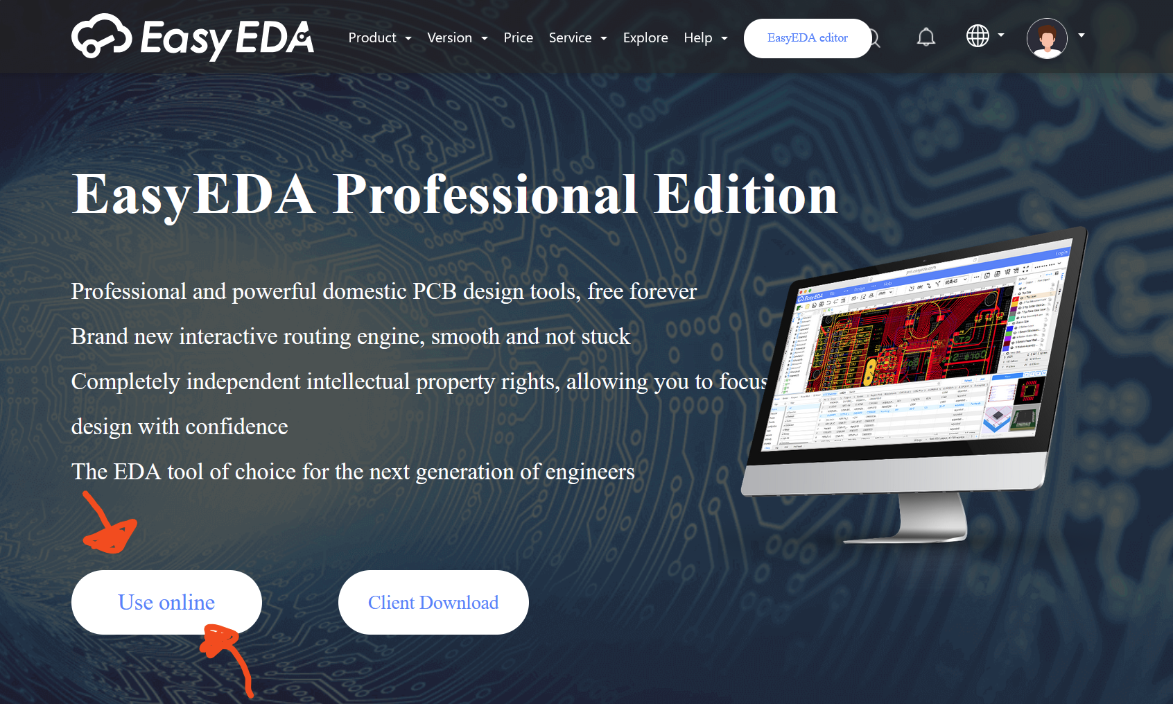
After creating an account and logging into EasyEDA, go to https://pro.easyeda.com/ and click Use Online, or directly visit https://pro.easyeda.com/editor.
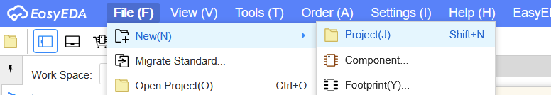
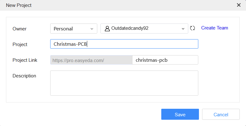
Next, go to File -> New -> New Project, name your project, and click Save.
Once saved, your project will automatically open. On the left sidebar, you’ll find both the schematic and PCB pages.
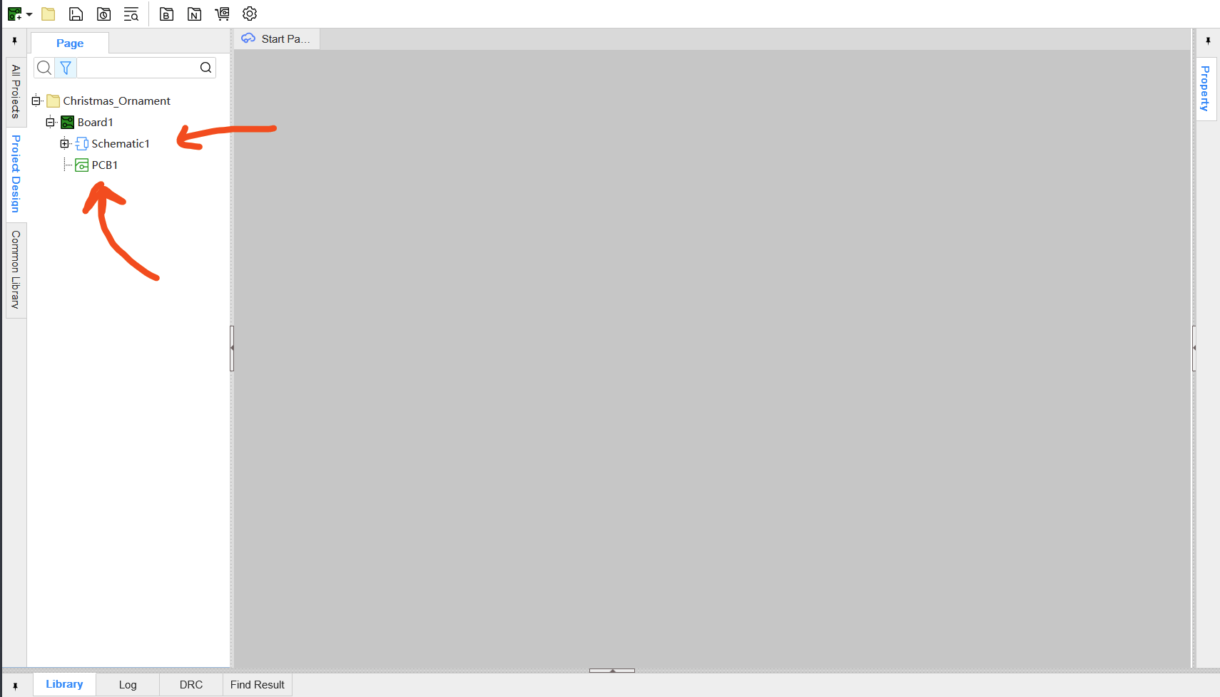
Double-click Schematic1 to open the schematic view.
For the sake of simplicity in this tutorial, we’ll skip adding any components like LEDs and resistors. Instead, we’ll head straight to the PCB editor to design the ornament itself.
Double-click PCB1 to open the PCB editor. You’ll see a blank canvas where you can design your PCB.
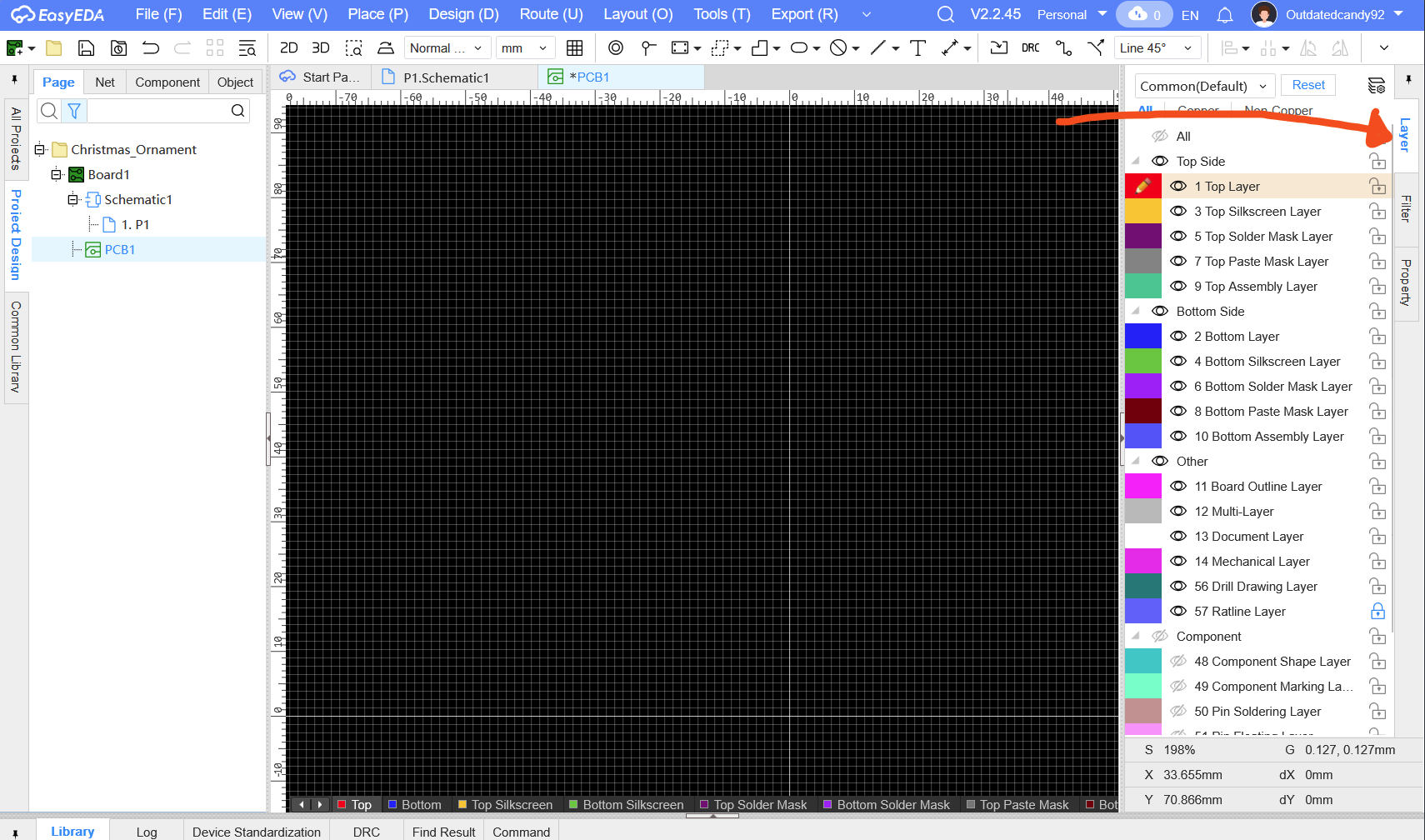
On the right sidebar, open the Layers panel. There are many layers listed, but for this tutorial, we’ll focus on three main ones:
- Board Outline Layer
- Top Silkscreen Layer
- Bottom Silkscreen Layer
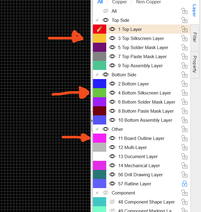
Board Outline Layer: Defines the physical shape and size of your PCB, including any cutouts or slots. This layer tells the manufacturer exactly where to cut.
Top Silkscreen Layer: Prints component labels, decorations, or logos on the top of the board. For your ornament, this is where most of your visual design will appear.
Bottom Silkscreen Layer: Prints labels or designs on the underside of the PCB. Useful for double-sided decorations or additional visual elements.
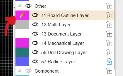
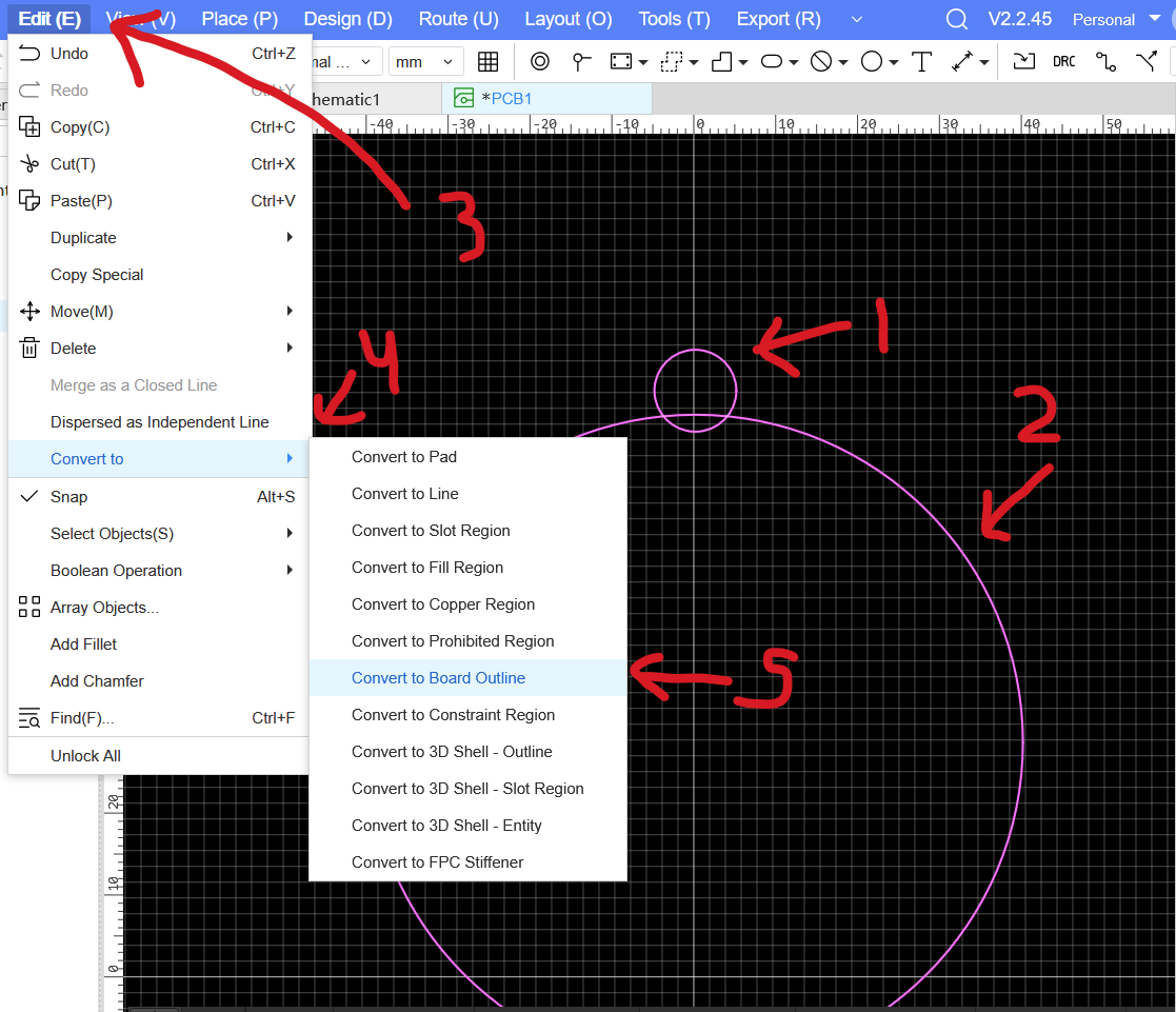
- Select the Board Outline Layer from the right sidebar.
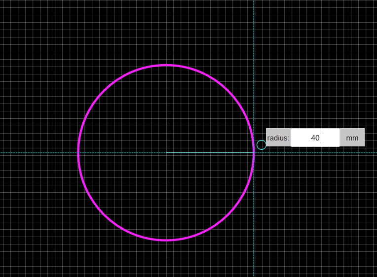
- From the top toolbar, choose the Line Tool. Click the dropdown and select Circle.
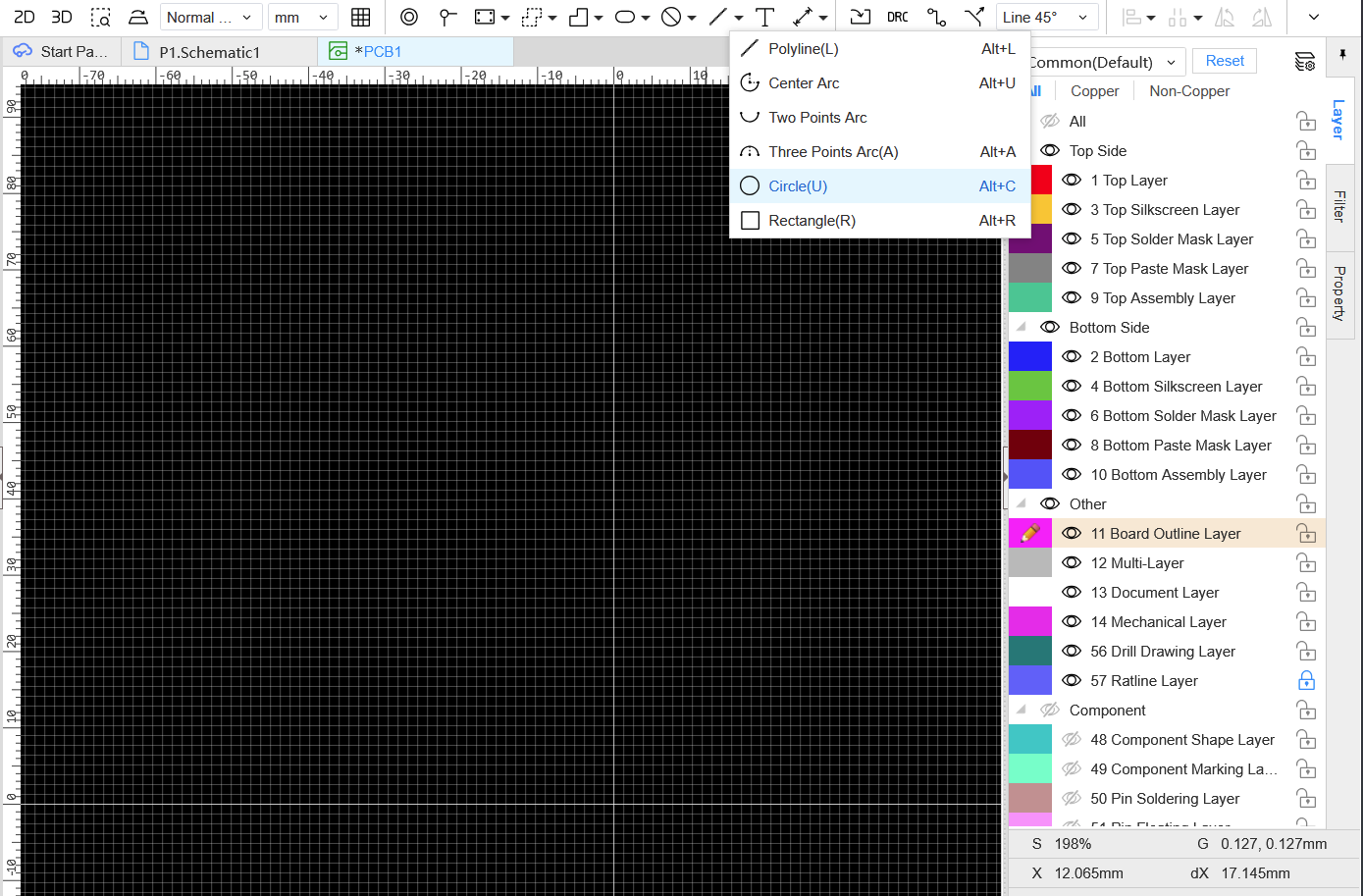
- Draw a large circle with a radius of 40 mm to serve as the ornament’s main body. Simply click anywhere and then enter 40 for the radius and press enter.
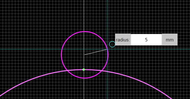
- Create a smaller circle with a 5 mm radius, this will form the hole at the top for hanging.
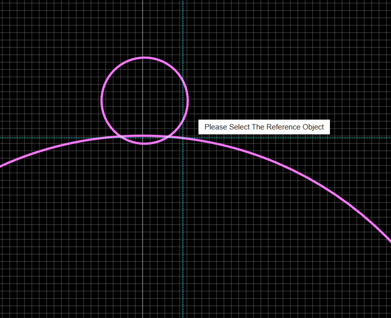
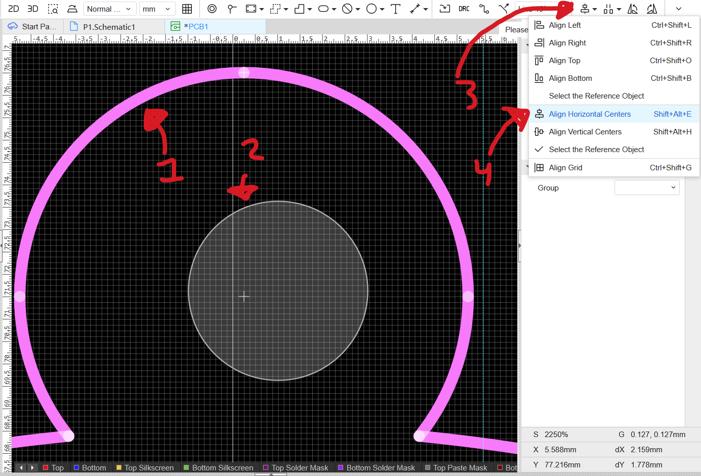
- Select both circles and align them horizontally.
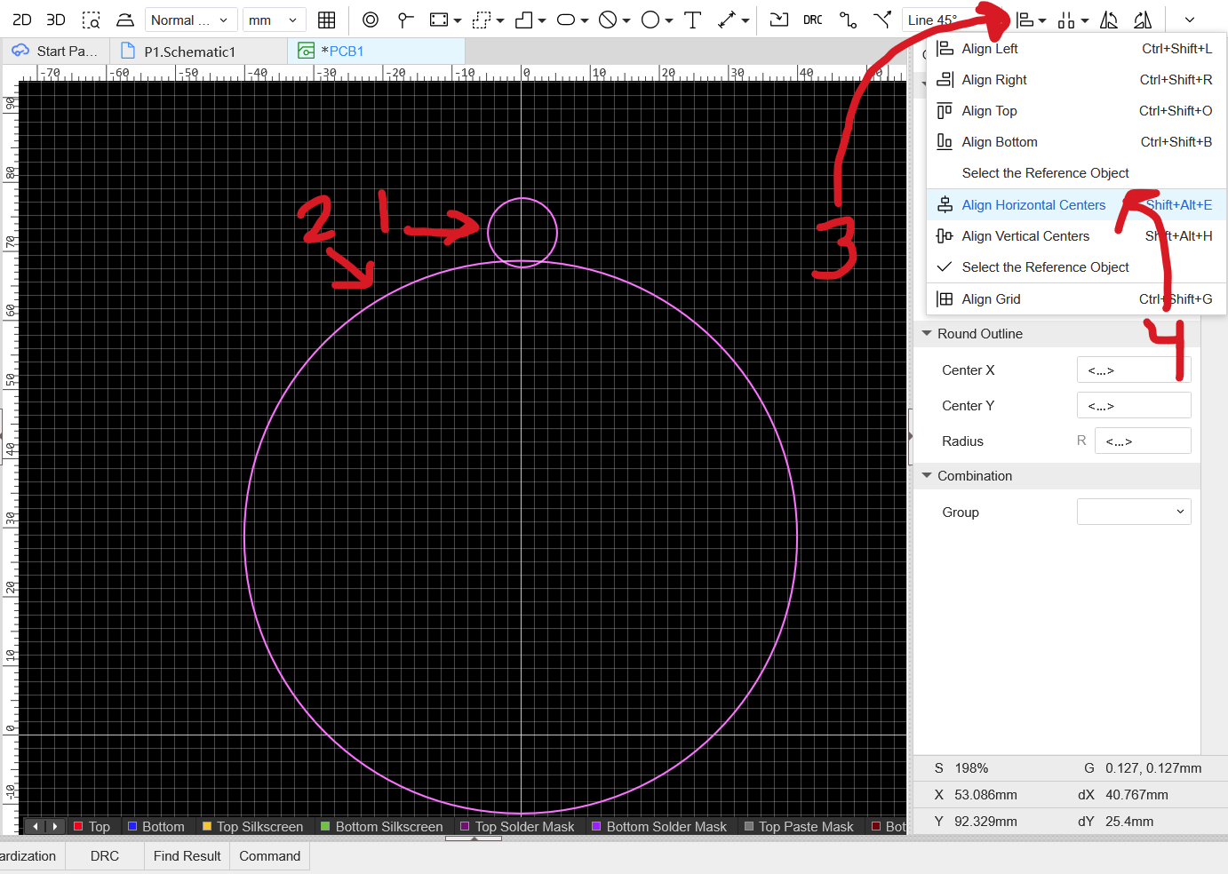
- It will ask then you to select The Reference Object. Simply click on one of the circles
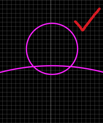
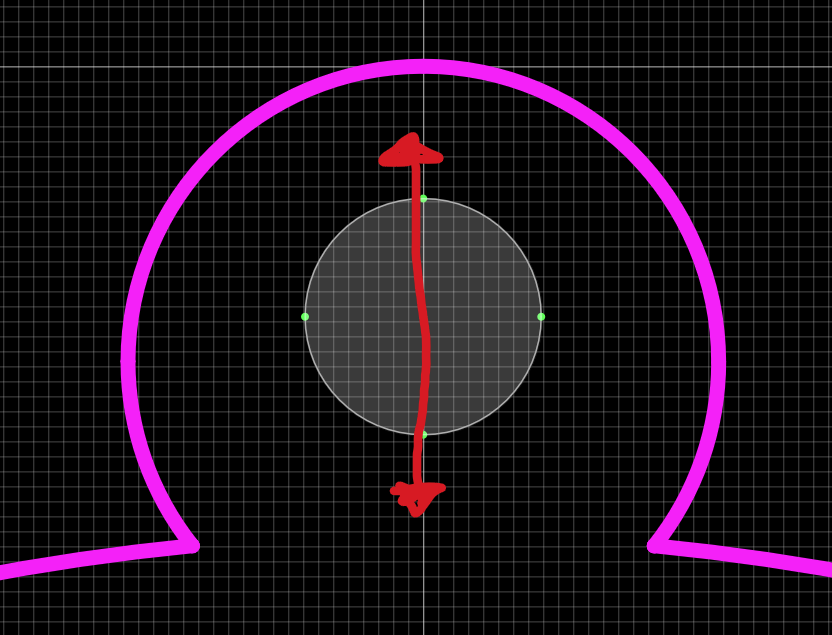
- Move the smaller circle to move it slightly on the top edge of the larger circle. Hold Shift will moving it so that it only moves in one dimension.
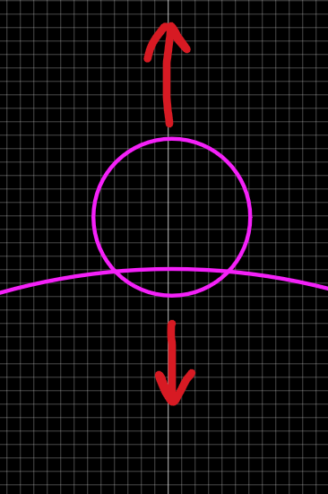
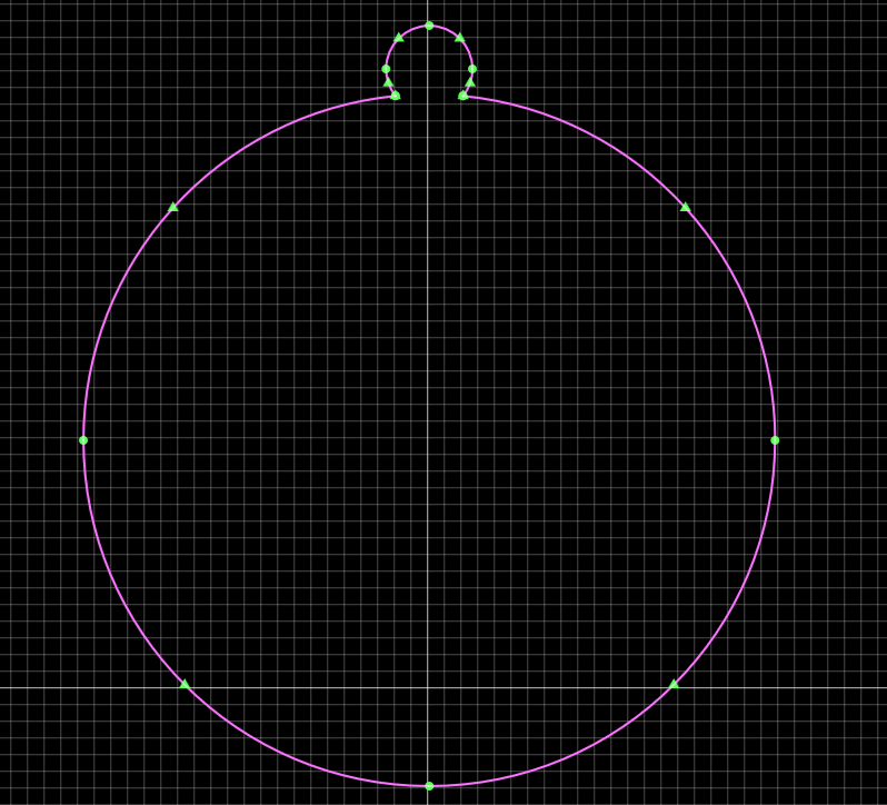
Here's how it should look like after you move it
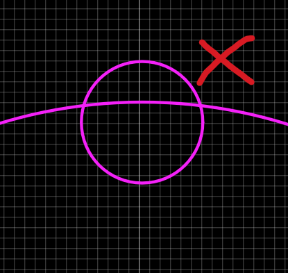
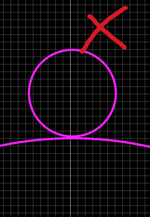
It should NOT be like this
- Now select both circles, go to
Edit -> Convert To -> Board Outline.
It should look like this after you do this step
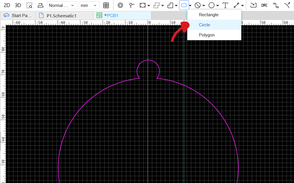
- Next, create a Slot Zone with a 2 mm radius.
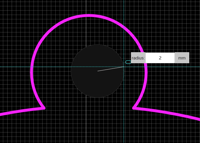
- Center the slot vertically by selecting both objects and choosing Horizontally Center.
- Hold Shift and drag the slot region up or down as needed until it’s well positioned and looks vertically centered inside the small circle.
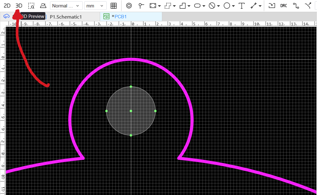
Click the 3D button to preview your PCB. You should now see the 3D render of your ornament outline.
Now lets head back into the PCB editor and add some cool designs
Before importing any artwork, let’s ensure that the Multicolor Silkscreen feature is enabled.
- Go to Settings -> PCB -> General.
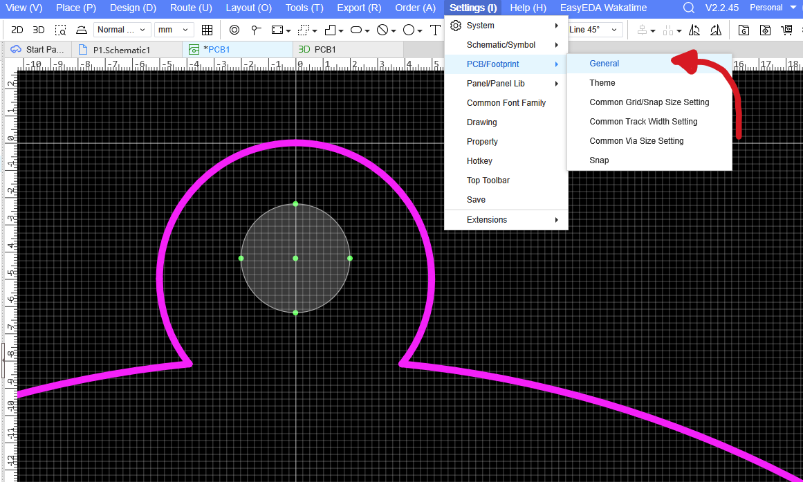
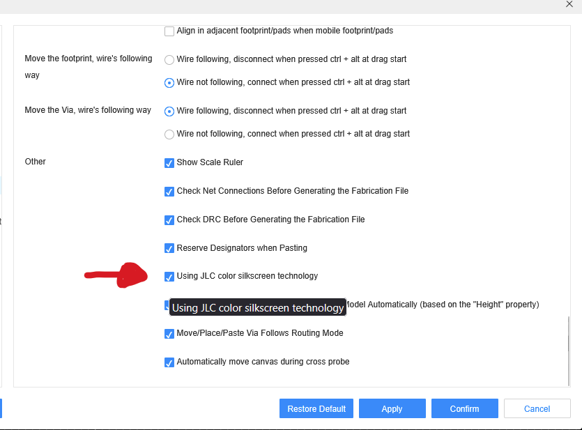
- Scroll down to find Using JLC Color Silkscreen Technology.
- Make sure it’s enabled, then click Confirm.
Now you can add your own artwork:
- Go to
File -> Import -> Image.
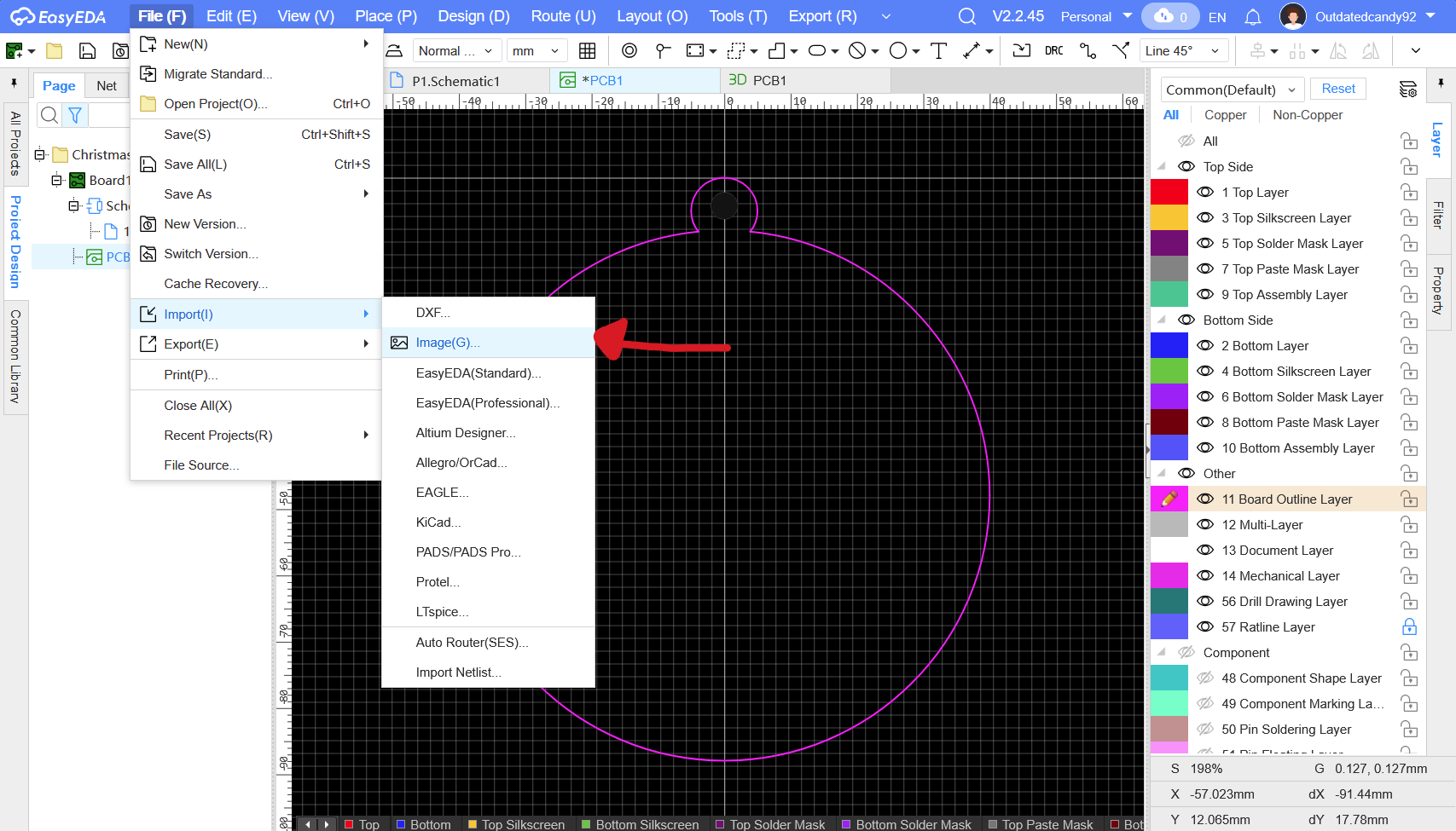
- In the Insert Image dialog, check Place Original Image.
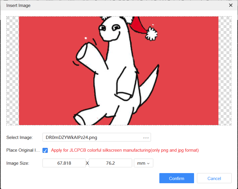
- If your image file is large, set the image size to under 90 mm .you can always scale it later in the editor.
Tips:
- Use high-quality 300 PPI PNG or JPG files for best results.
- Avoid low-resolution images, as they may appear pixelated during printing.
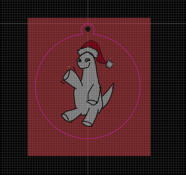
Once imported, position the image wherever you’d like on the board. By default, it will appear on the Top Silkscreen Layer. Make sure to scale up your image so that it's background overflows out of the PCB.
Tip: You can hold shift while scaling to ensure it's ratio is consistent
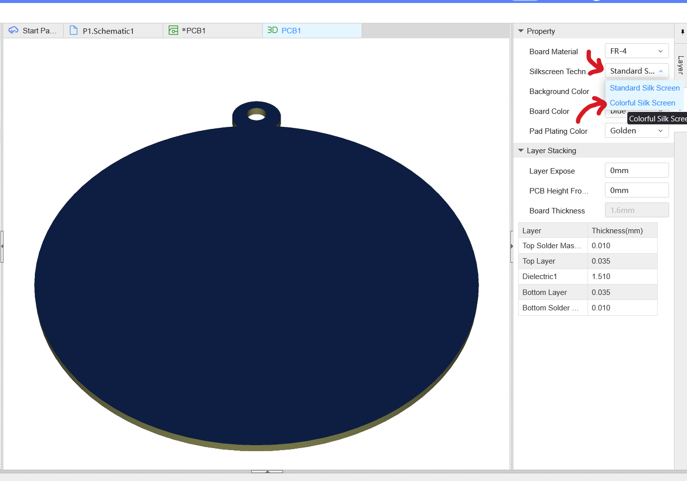
To preview how your PCB looks click on the 3D Preview again , select Colorful Silkscreen as the silkscreen technology under the PCB editor settings.
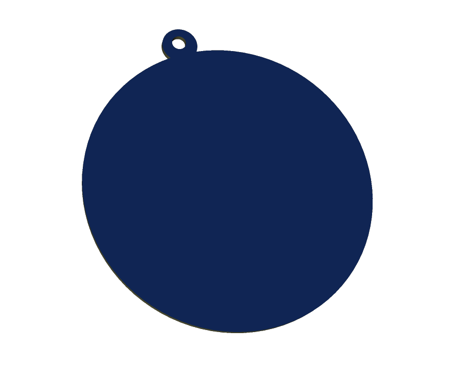
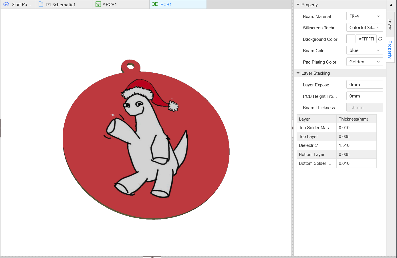
This is how it should finally look
If you’d like to add designs on the back of the PCB, simply:
- Click the image you imported.
- In the Properties panel, change the Layer dropdown to Bottom Silkscreen Layer.
- Adjust placement as desired.
Once you’re happy with your design, it’s time to generate the files and place your order.
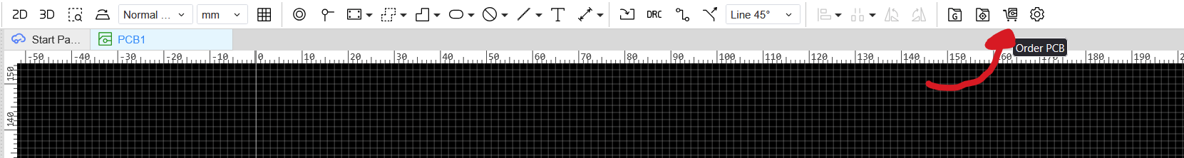
- In the PCB editor, Go on the top bar and click on the order PCB icon
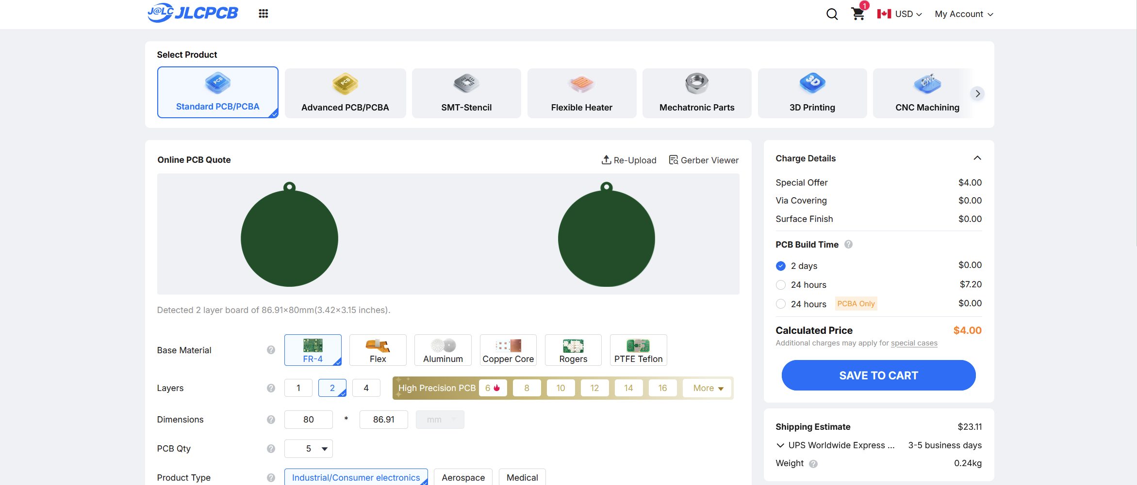
You're going to get a bunch of dialogs, just continue and it will then take you over to JLC
- You will see something like this on the order page
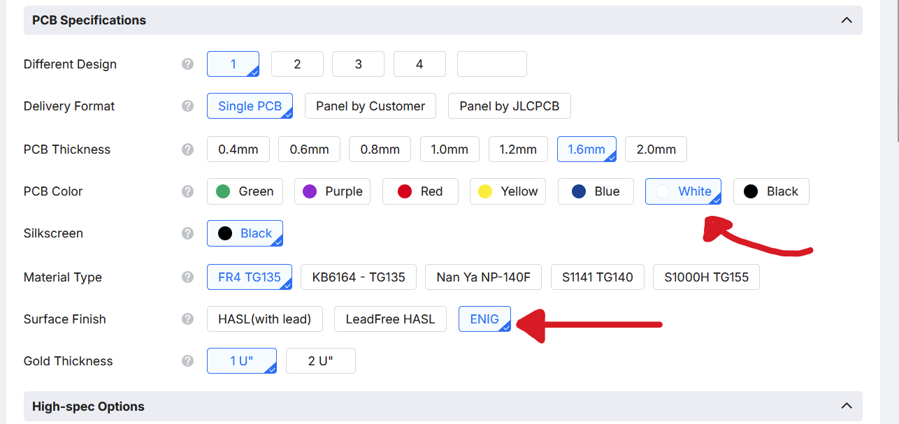
- Change your settings as shown
Under PCB Specifications change PCB Color to White and Surface Finish to ENIG
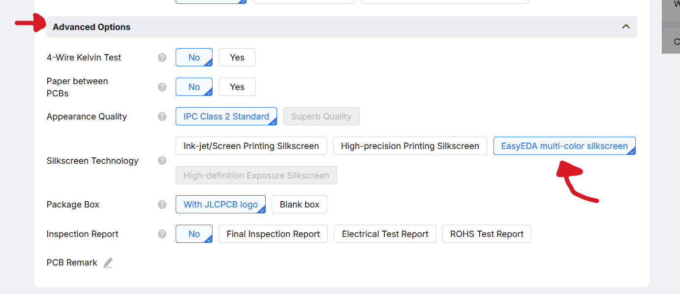
Then scroll down and open advanced options dropdown and select EasyEDA multi-color silkscreen as your Silkscreen Technology
After that just add it to your cart and you should be all set!
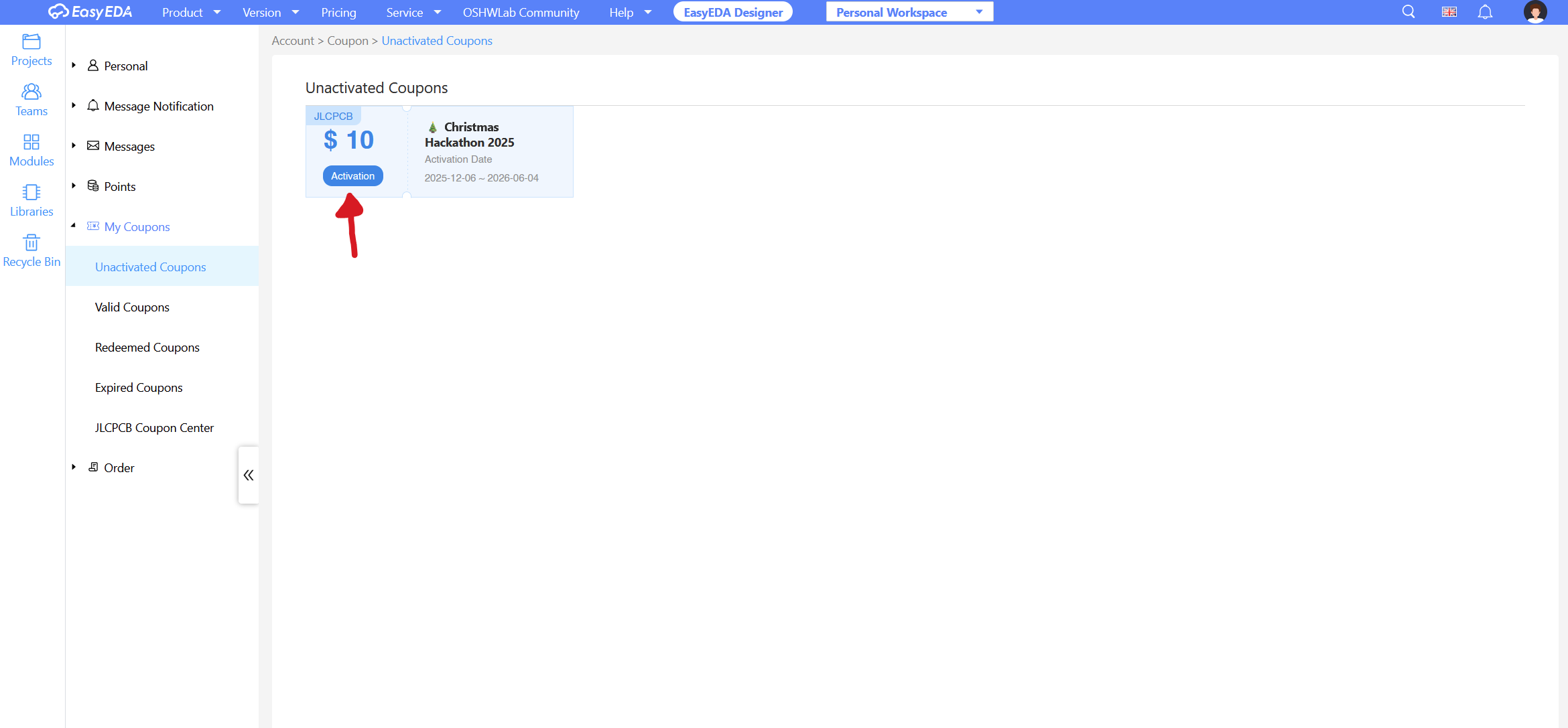
- Click here to claim a $10 coupon which you can use towards your board.
Make sure to activate the coupon!
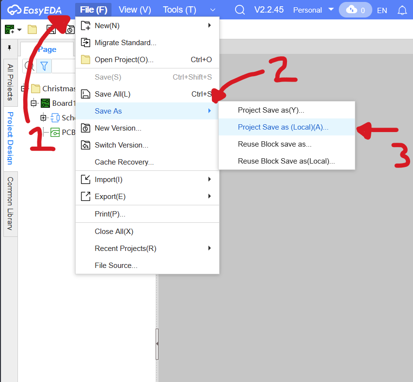
- Export your source files!
Go to file -> Save as -> Project Save as (Local) This should give a .epro file.
-
Create a GitHub repository and upload the .epro file
-
Head over to the Submit Form and submit your project. (For the Playable URL you can just use your GitHub URL)
-
Now simply wait for a few days to get your grant! Once you get the grant you can order your PCB :D