In this project we are going to implement the HACK computer designed in parts I and II of the Nand2Tetris course.
For the HACK computer itself we will be using a DE10-Lite FPGA board from Terasic. It is available for purchase from their website for around $80 along with many expansion interface, multimedia, video/imaging, networking, AD/DA, robotics boards. It is also freely available on ebay. The board is built around the Altera MAX 10 10M50DAF484C7G chip with 50,000 logic elements, 1,638 Kb of on-chip memory, 64MB of SDRAM, 2x20 GPIO interface and a VGA interface.

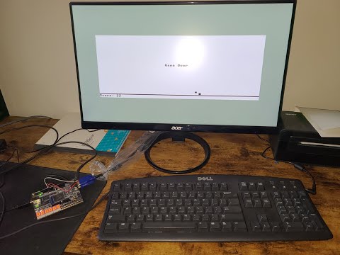
And for the peripherals we will need a VGA monitor with a cable and a PS/2 keyboard.
In part I of the course we designed the HACK computer using a hardware definition language designed by the authors. Now we need to implement it in a real HDL. There are 2 options to choose from: Verilog and VHDL. Which one is better is a subject of a thirty years' holy war, but if you don't already have a favourite I suggest Verilog for its shallower learning curve and simpler syntax.
In part I we used structural design patterns to implement system logic. We chose a NAND gate as a basic building block, and then instantiated it inside higher modules to gradually create more complex functions. While this approach has its place in hardware design it isn't always the most effective. Take for example our ALU. To design it we first had to design AND, OR, XOR and NOT gates, along with their 16-bit versions. Then using these basic gates we designed a multiplexer and an 8-way OR gate, then tied them all together to get the required ALU functionality. Now compare all that code we had to write to the same ALU implemented in Verilog using behavioral modeling:
module alu (
    input  [15:0] x,    // input x (16 bit)
    input  [15:0] y,    // input y (16 bit)
    input         zx,   // zero the x input?
    input         nx,   // negate the x input?
    input         zy,   // zero the y input?
    input         ny,   // negate the y input?
    input         f,    // compute out = x + y (if 1) or x & y (if 0)
    input         no,   // negate the out output?
    output [15:0] out,  // 16-bit output
    output        zr,   // 1 if (out == 0), 0 otherwise
    output        ng    // 1 if (out < 0),  0 otherwise
);

  wire [15:0] xz = zx ? 16'h0000 : x;
  wire [15:0] xn = nx ? ~xz : xz;
  wire [15:0] yz = zy ? 16'h0000 : y;
  wire [15:0] yn = ny ? ~yz : yz;
  wire [15:0] outn = f ? (xn + yn) : (xn & yn);

  assign out = no ? ~outn : outn;
  assign zr  = (out == 16'h0000);
  assign ng  = out[15];

endmodule
Here we implemented the same logic as before in only 8 lines of code. And now it is the synthesis tool's job to generate the most efficient hardware realisation of this function.

DE10 Lite comes with a 50 MHz clock. We will need to step it down to 25 MHz for our project. In Quartus Prime we have PLLs available as free IP blocks, which we can instantiate with the required parameters. If you plan to sim this project with ModelSim make sure to include altera_mf_ver library which contains PLL's source code. PLL has about 20 ns lag, so we will tie our reset to its output.
  reg  [3:0] rst_cnt = 4'h0;
  wire       rst = ~rst_cnt[3];
  always @(negedge clk_25)
    if (~KEY[0] | ~locked) rst_cnt <= 4'h0;
else if (rst) rst_cnt <= rst_cnt + 1;In order to be able to run Pong, which compiles to 50,000 instructions, we need to make one small change to our CPU design. In the original specification we distinguish A from C instruction by the first MSB only. This limits the ROM address pool to only 32,768 instructions, which isn't enough for Pong. So in our design we will make a small change. Only instructions starting with 111 are now C-instructions and everything else will be A-instructions. This way we increase the ROM address pool to 57,343 while maintaining reverse compatibility with the original design.
wire cInstr = &instruction[15:13];For all our memory needs we will make 3 memory blocks and a bunch of individual registers to handle IO like switches and LEDs. For instruction memory we will make a ROM module consisting of 57,344 16-bit registers. We will initialize it with our os.hack file.
initial $readmemb("os/os.hack", MEM);Then we will make two separate modules for RAM and screen map. Since we have two separate modules, CPU and VGA controller, address screen map at the same time, we will make it dual-channel, read/write channel for CPU and read-only channel for VGA.
DE10 Lite comes with a 4-bit VGA DAC and supports standard VGA resolution 640x480 at 25MHz. Since Hack OS is designed to work with 512x256 resolution we will have to add a 128x224 frame to our picture.
You will need a PS/2 keyboard and a pigtail to connect it to GPIO. Connect it according to the diagram below.
| Signal | Keyboard pin | GPIO pin |
|---|---|---|
| Vcc | 4 | 11 |
| GND | 3 | 12 |
| DATA | 1 | 9 |
| CLK | 5 | 10 |

You can use five new OS functions to control button KEY1, 10 switches SW0 - SW9, 10 LEDs LEDR0 - LEDR9 and 6 7-digit displays HEX0 - HEX5.
class IO {
    function boolean button();
    function int sw();
    function void led(int number);
    function void seg(int number);
    function void status(int number);
}If you want to use my compiler, simply run make command if you have clang and make already installed (if you want to use gcc instead simply replace clang with gcc inside Makefile).
To synthesise and program our design to DE10 we will use Quartus Prime software from Intel. It has a free Lite version which is enough for our project. It also comes with a free simulation tool ModelSim. Since version 21 ModelSim was replaced with its advanced version Questa, which requires a license to run (it can be acquired for free for a year). I would recommend installing version 17 Lite, since it doesn't require any licenses to run. During installation make sure to select MAX10 Device support, Programmer, USB-Blaster drivers and ModelSim Starter Edition (if you want to be able to run simulation).
- Clone the project
git clone https://github.com/gunnerson/hack-fpga.git. - Start Quartus Prime and create a new project. For path specify the directory from [1]. For project name type
HACK. - For project type choose
Template. Go to Intel Design Store. In search typeDE10 Lite MAX10and downloadIntel® MAX® 10 FPGA – Terasic DE10-Lite Board Baseline Pinouttemplate. Back in Quartus clickInstall the design templateand add downloaded*.parfile. This will create all the necessary pin assignments and global parameters for us in the*.qsffile.
- Now we need to add our project files. Go to
Project -> Add/remove files. Click...next toFilefield, selecttop.vand clickOpen. Repeat for all files inv/directory. ClickOKto finish. - In the
Project NavigatorselectFilesinsteadHierarchy. Right-click ontop.vand pressSet as Top-Level Entity. You can deleteDE10_LITE_GOLDEN_TOP.vfrom project files now. - We need to add a PLL to generate a 25 MHz clock. In the
IP CatalogfindALTPLLand double-click it. Name itpll. Forinclk0frequency set 50 Mhz. On the next tab uncheckareset. On theOutput clockstab forclk c0enter output clock frequency 25 MHz. Leave everything else default. ClickFinishand agree to add*.qipfile to project. - Go to
Assignments -> Device -> Device and Pin Optionsand change configuration mode toSingle Uncompressed Image with Memory Initialization. - Compile Design. Make sure it completes without errors.
- Open Programmer. Select
USB-BlasterinHardware Setup. PressStart. Wait for the progress bar to reach 100%. Device is programmed. Pong should be running on the screen. You can use theKEY0button to restart Hack.