Simulating a fictional processor design and architecture using Java, by creating a Von Neumann Memory Architecture which is a digital computer architecture whose design is based on the concept of stored program computers where program data and instruction data are stored in the same memory.
Using Von Neumann Memory Architecture which is a digital computer architecture whose design is based on the concept of stored program computers where program data and instruction data are stored in the same memory.
- Memory Size = 2048 * 32
- The main memory addresses are from 0 to 211 − 1 (0 to 2047).
- The memory is word addressable
- Addresses from 0 to 1023 contain the program instructions. • Addresses from 1024 to 2048 contain the data.
-
Size: 32 bits
-
31 General-Purpose Registers (GPRS) – Names: R1 to R31
-
1 Zero Register – Name: R0 – Hard-wired value “0” (cannot be overwritten by any instruction).
-
1 Program Counter
– Name: PC
– A program counter is a register in a computer processor that contains the address (location) of the instruction being executed at the current time.
– As each instruction gets fetched, the program counter is incremented to point to the next instruction to be executed.
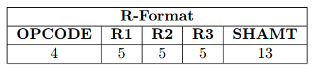
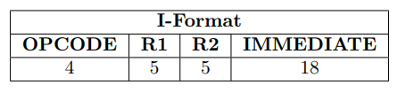
- We have 3 format (R-Format, I-Format, J-Format)
- R-Format:
- I-Format:
- J-Format:
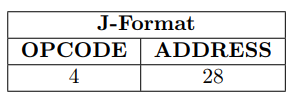
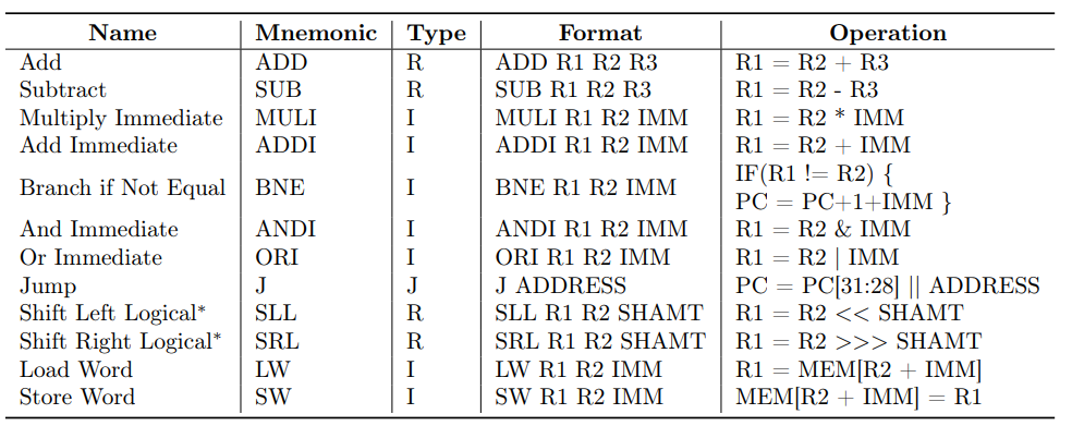
- The opcodes are from 0 to 11 according to the instructions order in the following table:
All instructions regardless of their type must pass through all 5 stages even if they do not need to access a particular stage.
- Instruction Fetch (IF): Fetches the next instruction from the main memory using the address in the PC (Program Counter), and increments the PC.
- Instruction Decode (ID): Decodes the instruction and reads any operands required from the register file.
- Execute (EX): Executes the instruction. In fact, all ALU operations are done in this stage.
- Memory (MEM): Performs any memory access required by the current instruction. For loads, it would load an operand from the main memory, while for stores, it would store an operand into the main memory.
- Write Back (WB): For instructions that have a result (a destination register), the Write Back writes this result back to the register file.
- 4 instructions (maximum) running in parallel
- Instruction Fetch (IF) and Memory (MEM) can not be done in parallel since they access the same physical memory. • At a given clock cycle, you can either have the IF, ID, EX, WB stages active, or the ID, EX, MEM, WB stages active. • Number of clock cycles: 7 + ((n − 1) ∗ 2), where n = number of instructions
– Imagine a program with 7 instructions: 7 + (6 ∗ 2) = 19 clock cycles
- Example for the Pipleline pattern:
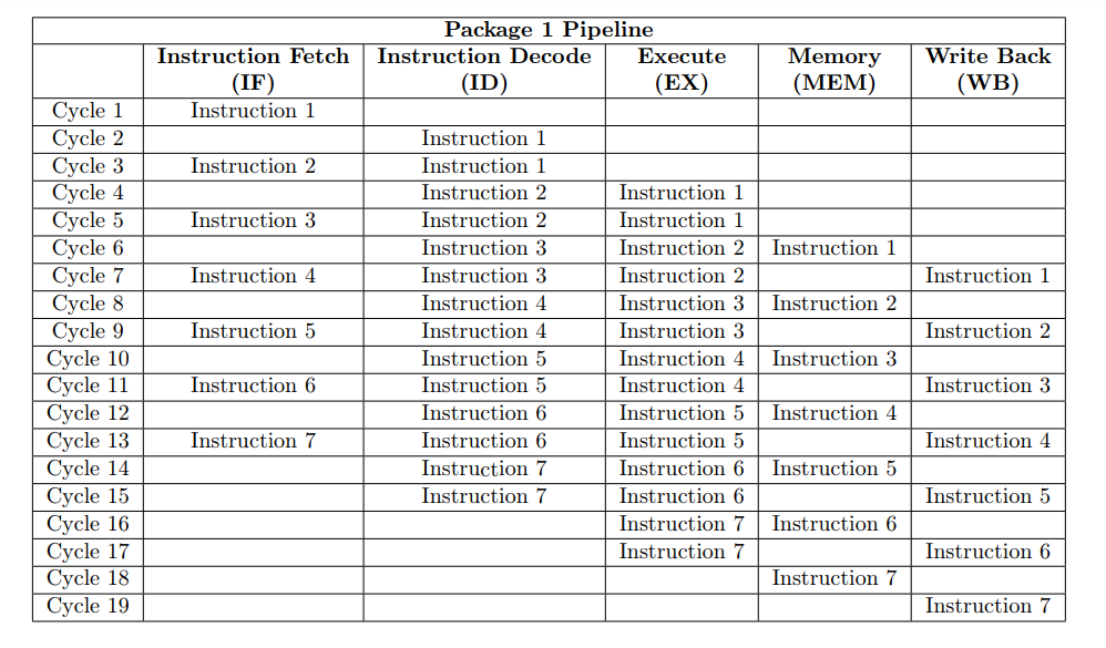
- The pattern is as follows:
*You fetch an instruction every 2 clock cycles starting from clock cycle 1.
- An instruction stays in the Decode (ID) stage for 2 clock cycles.
- An instruction stays in the Execute (EX) stage for 2 clock cycles.
- An instruction stays in the Memory (MEM) stage for 1 clock cycle.
- An instruction stays in the Write Back (WB) stage for 1 clock cycle.
- We cannot have the Instruction Fetch (IF) and Memory (MEM) stages working in parallel. Only one of them is active at a given clock cycle.
Project is created with:
- Java SE-15
- Eclipse IDE
- To run this project, just import the project as an existing project in Eclipse